Introduction
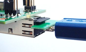

The purpose of the sfp2usb module is to allow the evaluation of the XillyUSB IP core on a wide range of popular development kits. It’s a low-cost passive adapter between an SFP+ interface and a micro-B USB 3.0 receptacle. Together with a commonly available cable, it connects the FPGA board to a computer’s USB 3.x port. This interfacing is difficult to make without an adapter, since virtually no development kit has a USB 3.x interface that goes directly to an MGT.
The SFP+ interface (consisting of a metal cage and a connector) is usually intended for fiber-optic transceivers. As such, this connector is wired directly to an MGT on the FPGA, with PCB routing on the development board that supports the MGT’s full range of bit rates. The sfp2usb module exposes these signals to the USB receptacle, with coupling capacitors and ESD protection components as required. Hence the module does no more than connecting the receptacle to the FPGA’s MGT, with signal integrity issues taken care of properly.
Insertion and removal
The module is pushed gently into the SFP+ cage, with the USB receptacle facing up in the same direction as the USB cage, until the plastic enclosure is in line with the cage’s edge. Attempting to insert the module incorrectly (wrong orientation and with reasonable force), will result in a partial insertion only.
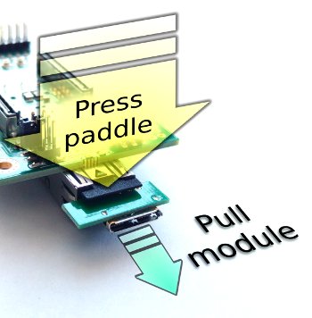
A retention mechanism prevents the module from accidentally being pulled out by the cable. It’s however not strong enough to withstand a forceful attempt of removal, which may damage this mechanism. Hence when removing the module from the SFP+ cage, press the small paddle under the PCB card against it (see picture to the right) to ease the removal and prevent mechanical damage to the retention latch.
Modules sold after February 2026 have a more rigid retention mechanism. With some SFP+ cages, it might be necessary to gently insert a toothpick between the paddle and the cage's retention flange (not deeper than 1mm) in order to release the module from the cage (see image to the right).
Electronic design
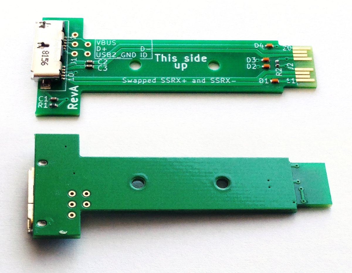
Click here to download the schematics for the sfp2usb module.
As seen in the schematics, there is a direct connection between the SuperSpeed signal pairs of the USB receptacle to the SFP+ finger pads, with coupling capacitors as required per specification. There are also ESD protection components on these wires. Note that the ground that is used is the one of the SuperSpeed signal set, and not the one used along with the USB 2.0 signals — even though they’re usually short-circuited by the link partner’s USB port.
The non-SuperSpeed pins of the USB receptacle are connected to testpoints on the board, with no particular intention of use. Some of these testpoints are not accessible when the PCB is inside its plastic enclosure.
In order to simplify the PCB layout (avoiding vias on the 5 Gb/s signal pairs), the differential signal pair towards the FPGA is swapped, so the bits are received by the FPGA with reverse polarity. The XillyUSB IP core has the capability of detecting and correcting reverse polarity of its arriving MGT bitstream (in fact, this capability is required per USB 3.x specification). Hence this swap has no impact with the XillyUSB IP core. There is however no need to make this swapping on a custom board, if it has no benefit to the PCB design.
The signal pair going from the FPGA (and driven by it) is not swapped. Hence the USB link partner has no indication of anything unusual.
The sfp2usb kit
The kit available for purchase consists of two elements:
- An sfp2usb module
- A USB 3.0 Micro-B male to Type-A male cable, 1 meter long.
The purpose of including a cable in the kit is not just convenience, but also to avoid low-quality cables, which may impact the low-level signal quality and consequently the overall user experience.