Introduction
The Xillybus IP core was designed with the understanding that data flow handling is where most FPGA engineers have a hard time, and is also a common reason for bugs. Fluctuations in the supply and consumption of application data tend to generate rarely reached states in the logic, often revealing hidden bugs which are extremely difficult to tackle.
Accordingly, Xillybus doesn't just supply a wrapper for the underlying transport (e.g. a PCIe DMA engine), but offers several end-to-end stream pipes for application data transport. This is a "once-and-for-all" solution, which has undergone heavy stress testing on numerous FPGA platforms and IP core configurations. Robustness and dependability can't be specified on a datasheet, but are easily told while testing. Luckily, integrating Xillybus with a target application for real-life stress testing is a relatively simple task, so evaluating its worthiness is a low-risk task with immediate results.
IP core functionality
Consider the following simplified block diagram, showing the application of one data stream in each direction (many more can be connected) for the PCIe-based Xillybus IP core. There is also a Xillybus IP core for AXI3 (targeting Zynq-7000 devices) as well as for USB 3.x (XillyUSB).
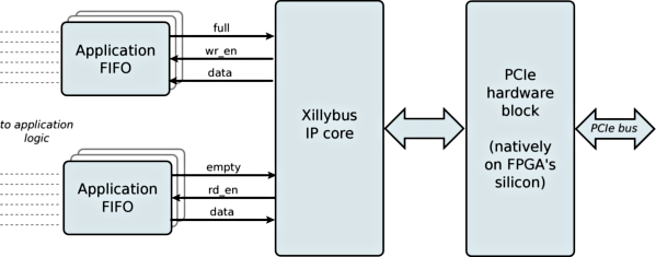
As shown in the figure above, the Xillybus IP core (the block in the middle) communicates data with the user logic through a standard FIFO ("Application FIFO" above), which is supplied by the IP core's user. This gives the FPGA designer the freedom to decide the FIFO's depth and its interface with the application logic.
This setting relieves the FPGA designer completely from managing the data traffic with the host. Rather, the Xillybus IP core checks the FIFOs "empty" and "full" signals in a round-robin manner, and initiates data transfers until the FIFOs becomes empty or full again (depending on the stream's direction).
On its other side, the Xillybus IP core is connected to the PCIe core supplied by AMD (formerly Xilinx) or Altera, as seen above.
To keep things simple, the Xillybus IP core has no knowledge about the expected data rate, and when the user logic is going to supply it or fetch it. Neither does it know about the FIFO's state, expect when it's empty or full. This makes the communication somewhat inefficient when the data rate is low, because small chunks are sent through the bus as soon as they reach the FIFO, rather than waiting for an application-specific chunk of information to arrive. The importance of this inefficiency is rather minimal, because it doesn't apply when the data rate increases. So all in all, Xillybus is efficient when it needs to be, and wastes bus transport resources when they're not used anyhow.
Despite the natural wish to take control of the DMA transactions and use the resources economically, there is little or no advantage in doing so. On the other hand, designing the DMA traffic according to a specific application makes the overall design stiff to modifications in the future, which is not the case for a plain FIFO setting.
Host driver functionality
The host driver generates device files which behave like named pipes: They are opened, read from and written to just like any file, but behave much like pipes between processes or TCP/IP streams. To the program running on the host, the difference is that the other side of the stream is not another process (over the network or on the same computer), but a FIFO in the FPGA. Just like a TCP/IP stream, the Xillybus stream is designed to work well with high-rate data transfers as well single bytes arriving or sent occasionally.
One driver binary supports any Xillybus IP core configuration: The streams and their attributes are auto-detected by the driver as it's loaded into the host's operating system, and device files are created accordingly. On Windows machines, these device files are accessed as \\.\xillybus_something. On Linux, they appear as /dev/xillybus_something.
Also when the driver loads, DMA buffers are allocated in the host's memory space, and the FPGA is informed about their addresses. The number of DMA buffers and their size are separate parameter for each stream. These parameters are stored in the FPGA IP core for a given configuration, and are retrieved by the host during the discovery process.
A handshake protocol between the FPGA and host makes an illusion of a continuous data stream. Behind the scenes, DMA buffers are filled, handed over to the other side and acknowledged. Techniques similar to those used for TCP/IP streaming are used to ensure an efficient utilization of the DMA buffers, while maintaining responsiveness for small pieces of data.
The size of the DMA buffers can be up to several gigabytes deep. As the data is stored in these buffers, the FIFOs inside the FPGA don't need to be large. Neither is there any real-time constraint on how often the user application software reads or writes data: The data keeps streaming from or to the DMA buffers even if the user application software is paused briefly for accessing the hard disk etc.
Conclusion
The Xillybus IP core offers both the FPGA engineer as well as the host application programmer with an interface which is probably the one both feel most comfortable with. While some PCIe bandwidth is wasted in certain occasions, the efficiency naturally rises with the demand for bandwidth, making these occasions of wasted bandwidth practically unnoticeable.
For those interested in how Xillybus is implemented internally, a brief explanation can be found in Appendix A of the programming guides for Linux or Windows.