Introduction
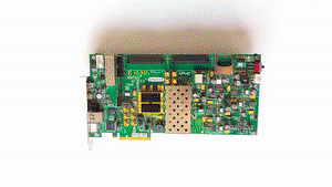
In the XillyUSB download page, there are FPGA design bundles for a variety of boards, most of which are official development kits. One exception is the Trenz TE0714-03-35-2I module, together with a TEBB0714 carrier board. This pair is an eligible choice in some scenarios, however it comes with a few obstacles. This page outlines some of them, along with the advantages of this choice.
Xillybus Ltd. is not affiliated with Trenz Electronic GmbH. This pair of boards was selected as they are suitable for small, low-budget FPGA projects involving XillyUSB:
- Available at below 150 USD (together).
- The TEBB0714 carrier board has an SFP+ cage, suitable for the sfp2usb module.
- The carrier board exposes many FPGA I/Os with a standard 0.1″ pitch through-hole interface. It’s hence easy to connect the FPGA I/Os to application electronics without professional soldering skills.
- The Artix-7 35T FPGA on the module board is large enough to contain the XillyUSB core and a typical FPGA project for the given amount of I/O.
Required additional hardware
Working with the Trenz module + carrier boards requires obtaining these two items separately:
- A JTAG programmer for Xilinx (often referred to as a “JTAG cable”). Unlike Xilinx’ development kits, which have an USB port and an on-board USB to JTAG controller, this is not the case with the Trenz solution.
- Power supply: Neither the Trenz module nor the carrier board arrive with one. A switched 3.3V / 3A power supply is recommended by the manufacturer.
To avoid confusion, it’s worth mentioning that for use with XillyUSB, the sfp2usb module also needs to be purchased separately. It’s also important to be aware that even though the XillyUSB IP core is available for download, it has certain licensing restrictions.
Working with TE0714-03-50-2I instead
At times, it might be difficult to purchase the TE0714-03-35-2I module due to shortage of this module. When this is the case, TE0714-03-50-2I can be used as a drop-in replacement. This module has a larger FPGA, and is accordingly slightly more expensive.
In order to target the FPGA design to the correct device, manually edit vivado-essentials/main.tcl in the downloaded bundle, and change the line saying
set thepart xc7a35t-csg325-2
to
set thepart xc7a50t-csg325-2
This change should be done before building the Vivado project by running the desired xillydemo-vivado.tcl script.
Hands-on notes
Neither the module nor the carrier board have a plug for the power supply. Rather, the voltage wires must be connected either pins or soldered directly to the carrier board. Section 5.2 of TEBB0714’s reference manual suggests several ways to connect the power supply.
A straightforward way is to use JX1, which is also used for connecting with the JTAG cable. All in all, the connections of JX1 are as follows:
- JX1/1 : GND from power supply
- JX1/5 : +3.3V from power supply
- JX1/2: GND from JTAG cable
- JX1/4: TCK from JTAG cable
- JX1/6: VREF from JTAG cable
- JX1/8: TDO from JTAG cable
- JX1/10: TDI from JTAG cable
- JX1/12: TMS from JTAG cable
Note that all the JTAG pins are on even pins (closer to the board’s edge).
For JTAG configuration to work, the configuration voltage needs to be set, possibly by installing a jumper between pins 3 and 4 of pin header J27, to enable the configuration voltage. This setting uses the module’s own voltage source. The red LED D3, next to JX1, indicates that the configuration voltage is present.
To set up the VCCO voltage for bank 34: Install a jumper between pins on J26. For example, for 3.3V on this bank, place the jumper between pins 5 and 6.
Another thing to note is that there are only three GPIO LEDs total: One on the module and two on the carrier board, all of which are used by the XillyUSB bundle (which normally requires four LEDs).