Introduction
This guide shows how to set up a Multi-Gigabit Transceiver (MGT) on an AMD (formerly Xilinx) Kintex-7 FPGA, and how to connect it to a Xillyp2p IP Core. In this example, a GTX is configured; however almost all details remain the same for other FPGAs in the 7-series family.
The example shown here is an implementation of the simplified application diagram shown on the guide about the IP core's ports and API:
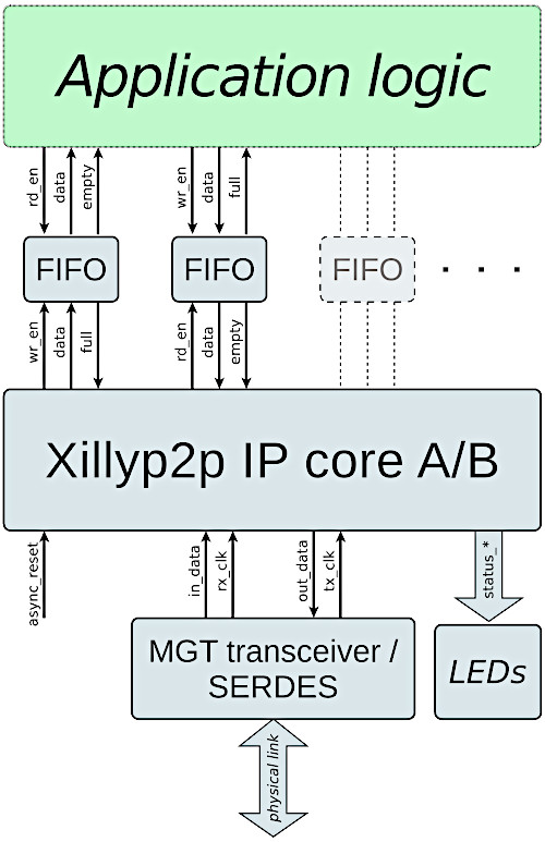
The interface between the GTX and Xillyp2p is very simple, as shown in detail above. Nevertheless, it can be quite challenging to configure the GTX correctly and determine how to connect its ports. A complete example of a working design, including screenshots, Verilog code and constraints, is given on this guide.
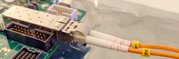
This example targets the KC705 board, which is the most popular development board for Kintex-7. The design presented here uses the board's SFP+ interface to connect with another board with the help of an optical transceiver module and an optical fiber, at a data rate of 5 Gb/s (connected as shown in the image above).
This design can be modified for other purposes and interfaces. As it uses the simplest possible GTX setup (without encoding), it's relatively easy to diagnose connectivity issues, if any arise. In addition, the Xillyp2p IP core has diagnostic output signals that can be connected to LEDs, as shown below. These can be helpful, particularly since one of the LEDs blinks for every bit error on the physical link.
For those interested in later AMD FPGAs (Ultrascale, Ultrascale+ and later), there's a separate guide showing how to set up an Ultrascale GTH, instead of the GTX used in this example.
Setting up the transceiver
The procedure is illustrated using screenshots and brief comments. This example was created with Vivado 2025.1, but it is compatible with other versions as well, possibly with only minor differences.
It's also possible to download a ready-made XCI file which reflects the configuration shown here.
In Vivado, open the IP Catalog and select 7 Series FPGAs Transceiver Wizard. Adjust the configuration according to the screenshots below. Note that the transceiver can be configured in more detail by accessing sub-menus within the Wizard; however, this is not necessary: Everything that needs to be changed is visible in the screenshots below. The Wizard's default configuration for "Start from scratch" is otherwise suitable.
The Wizard's initial window is the "GT Selection" tab, which should be configured as follows:
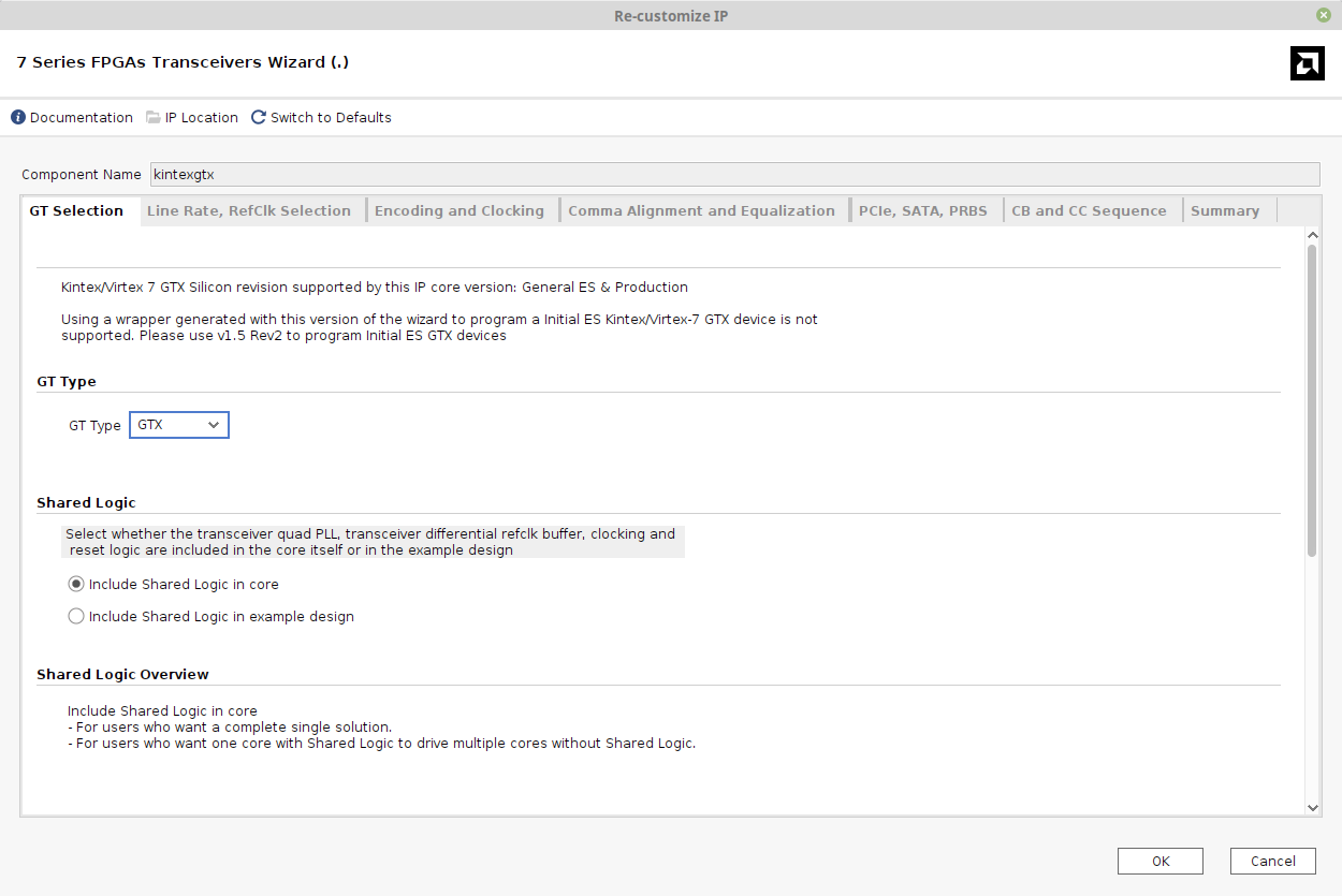
Things to modify:
- The IP's name is set to "kintexgtx". This is the name used in the instantiation in the Verilog example below.
- Select "Include Shared Logic in core". Note that the GT Type is "GTX", which is correct for Kintex-7. Other FPGAs in the 7-series family use different types; for example, Artix-7 uses GTP.
The next tab is "Line Rate, RefClk Selection", which looks like this:
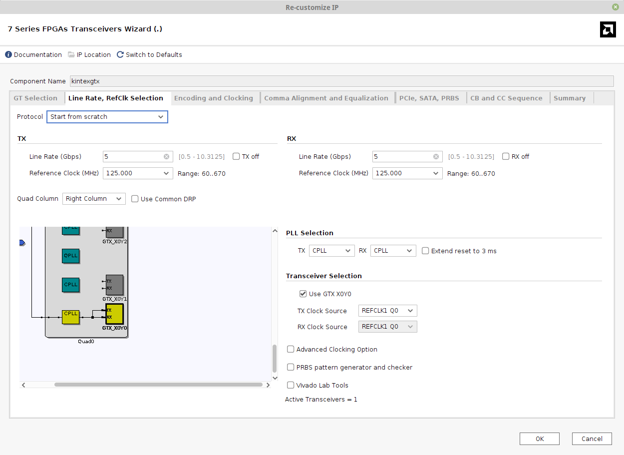
Things to pay attention to:
- The Line Rate is set to 5 Gb/s in both directions. You may want a different rate, depending on your equipment.
- The PLL type is chosen as CPLL for simplicity. This is a per-transceiver PLL, as opposed to Quad PLLs, which are shared among four transceivers and have richer features but are more complex to use.
- The "Actual Reference Clock" is the frequency of the external reference clock. On the KC705 board, a low-jitter 125 MHz clock source is supplied at pins G8/G7, so this clock is used.
The "Transceiver Selection" section allows choosing which of the FPGA's GTX resources are used. These settings are overridden by placements constraints in the project's XDC file, so this section has no effect on the final result. It's also possible to delete the constraints in the XDC file and rely on these settings. Which approach to use is a matter of preference; in this example, the Wizard's settings are ignored.
The next tab is "Encoding and Clocking":
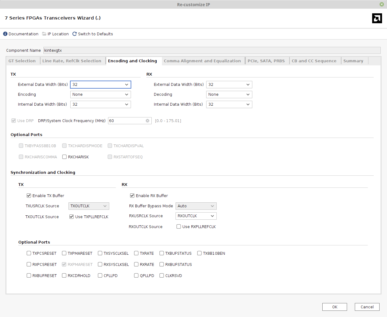
- "Encoding" remains at the default setting, Raw (no encoding), because Xillyp2p expects the transceiver to behave like a plain SERDES, without any manipulation of the data stream.
- Set External Data Width and Internal Data Width to 32 for both TX and RX. The External Data Width should match with the parallel word width specified for the Xillyp2p IP core.
- The DRP/System Clock Frequency should be changed to the frequency of the free-running clock in the design. This is an extra clock supplied to the transceiver for its housekeeping tasks. In this example, it's set to 60 MHz. An MMCM generates this clock, based upon the board's 200 MHz clock (see below).
- RXUSRCLK Source should be changed to RXOUTCLK.
The next tab is Comma Alignment and Equalization:
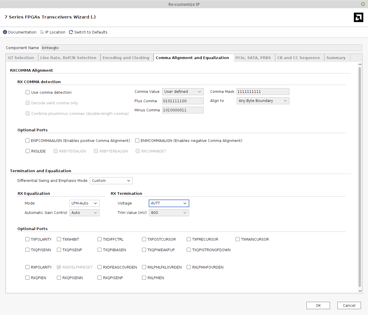
- Uncheck "Use comma detection". The transceiver's encoding feature is turned off, and Xillyp2p aligns the input data stream by itself.
- For RX Equalization, select LPM-Auto, enabling the next step.
- For RX Termination, the Voltage is set to AVTT. This sets the bias voltage applied at the GTX's electrical receiver inputs. If you are not using an optical fiber link with an SFP+ module, a different termination voltage may be preferable. This setting can dramatically affect link quality. Even if data arrives with many errors on every parallel word, adjusting the voltage can sometimes make the link completely error-free.
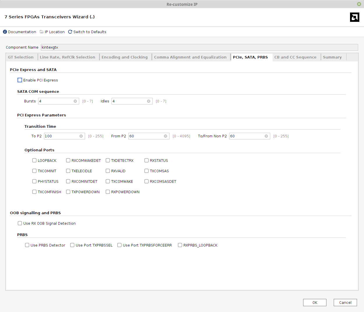
The next tab is "PCIe, SATA, PRBS". None of these features is enabled, so this tab can be skipped:
The following tab is "CB and CC Sequence", which can also be skipped:
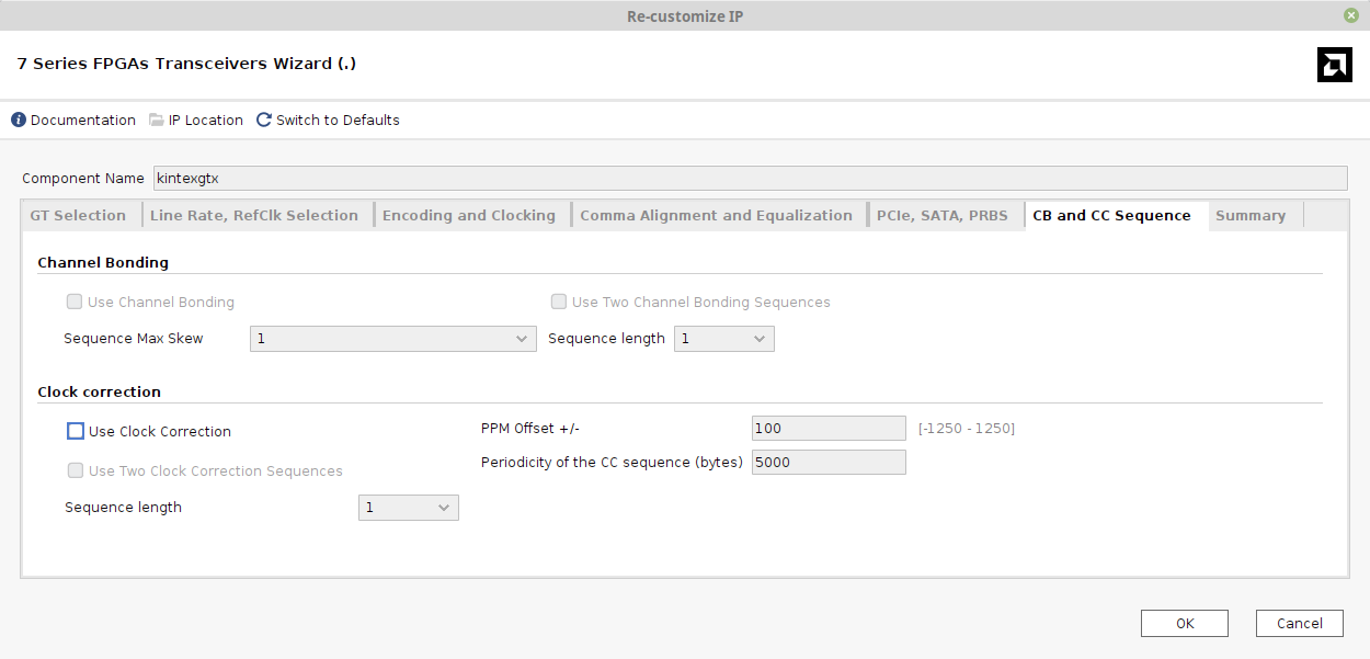
"Use Clock Correction" remains unchecked. Xillyp2p handles clock correction internally, and the transceiver cannot perform this task since encoding is disabled.
The last tab is a summary page, which looks like this:
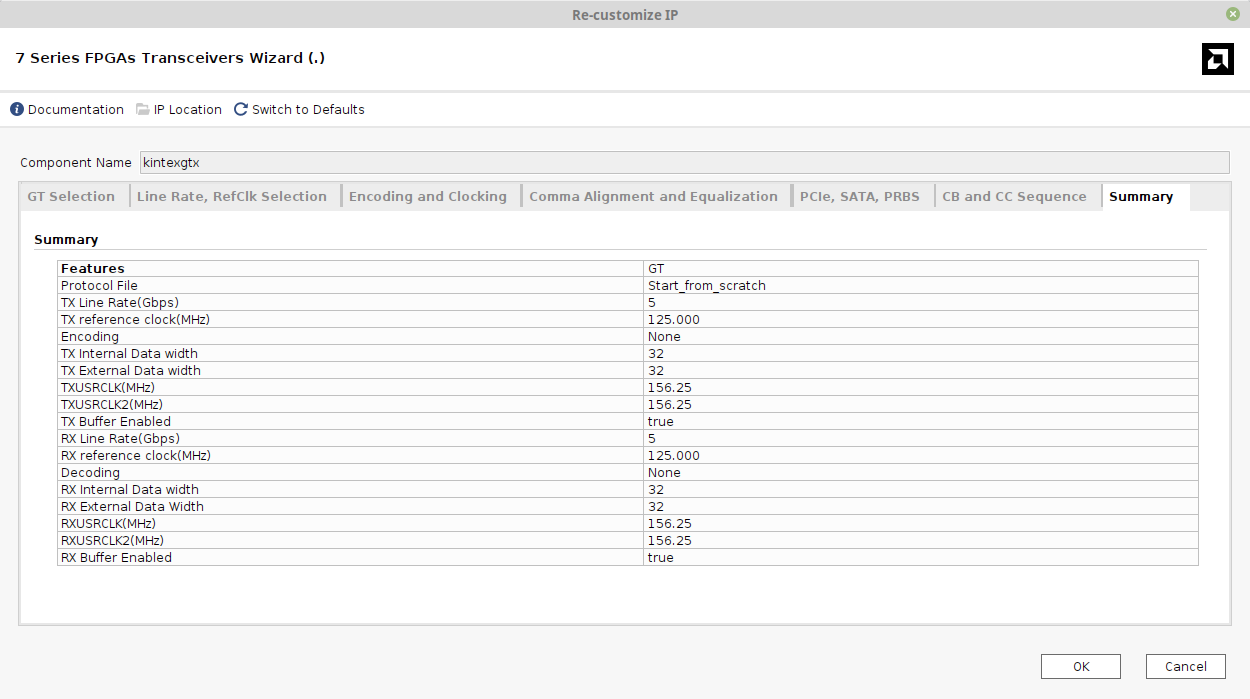
Note that unlike the example for Ultrascale, the clock frequency of tx_clk (TXUSRCLK2) and rx_clk (RXUSRCLK2) differ from the reference clock: tx_clk and rx_clk run at 156.25 MHz (the same as Ultrascale), but the reference clock is 125 MHz.
The configuration of the Xillyp2p IP core remains correct: The clock frequency specified there corresponds to tx_clk and rx_clk (156.25 MHz). The reference clock is only relevant for the transceiver's setup.
This concludes the setup of the GTX. Next, a sample Verilog design is shown.
Instantiation of transceiver
The example top-level Verilog module starts as follows:
module example
  (
   input  gtx_refclk_n,
   input  gtx_refclk_p,
   input  gtx_rxn,
   input  gtx_rxp,
   output gtx_txn,
   output gtx_txp,

   input  clk_200_p,
   input  clk_200_n,

   output sfp_tx_enable,

   output [7:0] gpio_led
  );
The first six ports belong to the GTX itself: The reference clock, the reception and transmission pins.
The clk_200_p/n ports are differential inputs for the KC705's free-running clock, which has a frequency of 200 MHz. sfp_tx_enable is explained briefly below.
Finally, there are eight LED outputs.
The connection between the transceiver and the Xillyp2p IP core is done in the same way as in the example for Ultrascale. The main difference is the instantiation of the transceiver.
Before the instantiation of the GTH itself, a free-running clock source is required. This is the instantiation of an MCMM that generates a 60 MHz clock from the 200 MHz clock that is supplied by the KC705 board:
  wire sysclk;
  wire pll_locked;

  syspll syspll_inst
   (
    .clk_in1_p(clk_200_p),
    .clk_in1_n(clk_200_n),

    .clk_out1(sysclk),

    .locked(pll_locked)
    );
Clocking Wizard is used to create syspll. The related XCI file is available for download.
These wires are required for interfacing with the Xillyp2p IP core:
  wire  rx_clk;
  wire  tx_clk;
  wire  async_reset;

  wire [31:0] in_data;
  wire [31:0] out_data;

  assign async_reset = 0;
async_reset is tied low in this example. This is somewhat careless, but the design works nonetheless. In a real-life design, it's recommended to use this asynchronous reset to reset the logic immediately after powerup.
Next, a small but possibly important detail:
assign sfp_tx_enable = 1; // Enable SFP+ transmitter
The sfp_tx_enable output port is connected to the optical transceiver's TX_DISABLE input through a MOSFET transistor, which negates its polarity. By default, there's a jumper installed on the board that keeps the transceiver's transmitter enabled. However, if this jumper is missing, the transceiver's transmitter will be turned off. By holding this output high, TX_DISABLE is forced low, ensuring that the optical transceiver operates normally.
Now to the instantiation of the transceiver:
   kintexgtx kintexgtx_i
     (
      .soft_reset_tx_in(!pll_locked), // Input is asynchronous
      .soft_reset_rx_in(!pll_locked), // Input is asynchronous
      .dont_reset_on_data_error_in(1'b1),
      .q0_clk1_gtrefclk_pad_n_in(gtx_refclk_n),
      .q0_clk1_gtrefclk_pad_p_in(gtx_refclk_p),
      .gt0_tx_fsm_reset_done_out(),
      .gt0_rx_fsm_reset_done_out(),
      .gt0_data_valid_in(1'b1),

      .sysclk_in(sysclk),

      .gt0_txusrclk_out(),
      .gt0_txusrclk2_out(tx_clk),
      .gt0_rxusrclk_out(),
      .gt0_rxusrclk2_out(rx_clk),

      .gt0_rxdata_out                 (in_data),
      .gt0_txdata_in                  (out_data),

      .gt0_gtxrxp_in                  (gtx_rxp),
      .gt0_gtxrxn_in                  (gtx_rxn),

      .gt0_gtxtxn_out                 (gtx_txn),
      .gt0_gtxtxp_out                 (gtx_txp),

      // Unused ports:

      .gt0_cpllfbclklost_out          (),
      .gt0_cplllock_out               (),
      .gt0_cpllreset_in               (1'b0),

      .gt0_drpaddr_in                 (9'd0),
      .gt0_drpdi_in                   (16'd0),
      .gt0_drpdo_out                  (),
      .gt0_drpen_in                   (1'b0),
      .gt0_drprdy_out                 (),
      .gt0_drpwe_in                   (1'b0),

      .gt0_dmonitorout_out            (),

      .gt0_eyescanreset_in            (1'b0),
      .gt0_rxuserrdy_in               (1'b0),

      .gt0_eyescandataerror_out       (),
      .gt0_eyescantrigger_in          (1'b0),


      .gt0_rxdfelpmreset_in           (1'b0),
      .gt0_rxmonitorout_out           (),
      .gt0_rxmonitorsel_in            (2'b00),

      .gt0_gtrxreset_in               (1'b0),
      .gt0_rxpmareset_in              (1'b0),

      .gt0_rxresetdone_out            (),

      .gt0_gttxreset_in               (1'b0),
      .gt0_txuserrdy_in               (1'b0),

      .gt0_txoutclkfabric_out         (),
      .gt0_txoutclkpcs_out            (),

      .gt0_txresetdone_out            (),

      .gt0_qplloutclk_out(),
      .gt0_qplloutrefclk_out()
      );
The transceiver is directly connected to the physical pins gth_rxp, gth_rxn, gth_txp and gth_txn. Unlike the GTH example, the reference clock's buffer is included within the transceiver module, so gtx_refclk_p and gtx_refclk_n are connected directly to the transceiver module as well.
The free-running 60 MHz sysclk is connected to sysclk_in. As mentioned above, this clock is used for the transceiver's control logic, including initialization. Because it takes a short period for the MMCM to lock to its 200 MHz reference clock, the negated pll_locked signal is used to reset the transceiver. This ensures that initialization begins only after sysclk is stable.
Note that tx_clk and rx_clk are outputs from the transceiver. In other words, the transceiver provides these two clocks through the gt0_txusrclk2_out and gt0_rxusrclk2_out ports. Together with in_data and out_data, these are the only connections between the transceiver and the Xillyp2p IP core, as shown next.
Instantiation of the Xillyp2p IP core
For this example, core A of an IP core that was generated at the IP core Factory is applied. Core B should be used on the other side of the physical link (unless the core is symmetric, a topic explained at the end of the guide about the IP Core Factory).
The configuration of the IP core is as shown in this screenshot from the web application:
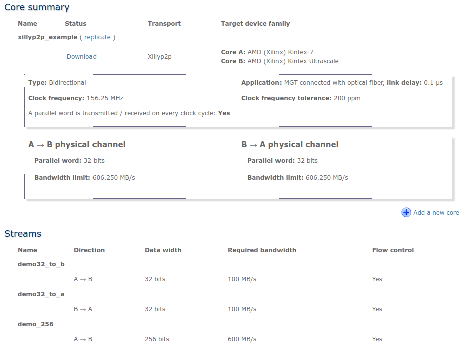
The general parameters of the IP core match those of the GTX: A 32-bit parallel word and a clock frequency of 156.25 MHz. Note that this is the frequency of rx_clk and tx_clk, and not the one of the reference clock. If, for example, the GTX' Line Rate is changed (without changing the reference clock and the width of the parallel word), the frequency of rx_clk and tx_clk will change accordingly. In that case, the updated frequency should be specified at the IP Core Factory.
Three streams were defined for this IP core: demo32_to_b, demo32_to_a and demo_256. A different number of streams, with different names and attributes can be configured as required for the application.
Before instantiating the IP core, a few additional wires are required. The following code segment is copied directly from the IP core's instantiation template:
  wire  status_link_down;
  wire  status_initializing;
  wire  status_link_partner_mismatch;
  wire  status_bit_error;
  wire  status_rev_polarity;
  wire [31:0] status_debug;

  wire [2:0] error_test_rate;

  // Wires related to data stream "demo32_to_a"
  wire  user_rx_demo32_to_a_wr_en;
  wire [31:0] user_rx_demo32_to_a_wr_data;
  wire  user_rx_demo32_to_a_full;
  wire  user_rx_demo32_to_a_eop;

  // Wires related to data stream "demo32_to_b"
  wire  user_tx_demo32_to_b_rd_en;
  wire [31:0] user_tx_demo32_to_b_rd_data;
  wire  user_tx_demo32_to_b_empty;
  wire  user_tx_demo32_to_b_eop;

  // Wires related to data stream "demo_256"
  wire  user_tx_demo_256_rd_en;
  wire [255:0] user_tx_demo_256_rd_data;
  wire  user_tx_demo_256_empty;
  wire  user_tx_demo_256_eop;
And now to the instantiation itself. This part too is copied from the instantiation template for core A:
  xillyp2p_core_a xillyp2p_core_a_ins (
    // Ports related to data stream "demo32_to_a"
    // Inbound data stream:
    .user_rx_demo32_to_a_wr_en(user_rx_demo32_to_a_wr_en),
    .user_rx_demo32_to_a_wr_data(user_rx_demo32_to_a_wr_data),
    .user_rx_demo32_to_a_full(user_rx_demo32_to_a_full),
    .user_rx_demo32_to_a_eop(user_rx_demo32_to_a_eop),

    // Ports related to data stream "demo32_to_b"
    // Outbound data stream:
    .user_tx_demo32_to_b_rd_en(user_tx_demo32_to_b_rd_en),
    .user_tx_demo32_to_b_rd_data(user_tx_demo32_to_b_rd_data),
    .user_tx_demo32_to_b_empty(user_tx_demo32_to_b_empty),
    .user_tx_demo32_to_b_eop(user_tx_demo32_to_b_eop),

    // Ports related to data stream "demo_256"
    // Outbound data stream:
    .user_tx_demo_256_rd_en(user_tx_demo_256_rd_en),
    .user_tx_demo_256_rd_data(user_tx_demo_256_rd_data),
    .user_tx_demo_256_empty(user_tx_demo_256_empty),
    .user_tx_demo_256_eop(user_tx_demo_256_eop),

    // General signals
    .rx_clk(rx_clk),
    .tx_clk(tx_clk),
    .async_reset(async_reset),
    .in_data(in_data),
    .out_data(out_data),
    .status_link_down(status_link_down),
    .status_initializing(status_initializing),
    .status_link_partner_mismatch(status_link_partner_mismatch),
    .status_bit_error(status_bit_error),
    .status_rev_polarity(status_rev_polarity),
    .status_debug(status_debug),
    .error_test_rate(error_test_rate)
  );

  // error_test_rate should always be zero unless you want to the test
  // what happens when there are errors on the physical data link.

  assign error_test_rate = 3'd0;
As mentioned before, the IP core connects with the GTX using four wires: rx_clk, tx_clk, in_data and out_data. The remaining connections are related to the application logic, as discussed next.
Exchanging data with the application logic
Those who have used Xillybus' IP core for PCIe or XillyUSB will find this part very familiar.
First, recall from above that this example revolves around core A, and that core B should (in general) be used on the FPGA on the opposite side of the physical link.
The application data stream named "demo32_to_a" allows the FPGA on the other side (with core B) to send data to the FPGA with core A.
The mainstream method to access this data is through a FIFO. For example, fifo_32 is a standard dual-clock FIFO with a 32 bit wide data word, defined in the Vivado project, and instantiated as follows:
   fifo_32 data_in_fifo
     (
      .rst(async_reset),
      .wr_clk(tx_clk),
      .rd_clk(<connect to application logic>),

      .din(user_rx_demo32_to_a_wr_data),
      .wr_en(user_rx_demo32_to_a_wr_en),
      .full(user_rx_demo32_to_a_full),

      .rd_en(<connect to application logic>),
      .dout(<connect to application logic>),
      .empty(<connect to application logic>)
      );
The three wires named user_rx_demo32_to_a_* are connected to the Xillyp2p IP core. The IP core uses these signals to fill the FIFO with data arriving from core B.
Note that the FIFO's "full" port is also connected. The Xillyp2p IP core respects this signal and avoid causing an overflow, by virtue of its flow control mechanism. This mechanism is optional but recommended (note that it says "Yes" on the "Flow control" column in the IP core's configuration screenshot for all three streams).
The FIFO's remaining ports are connected to the application logic, which retreives the data as needed. The application logic isn't required to fetch data at a certain rate; the only requirement is to avoid attempting to read from the FIFO when it's empty.
Also note that the FIFO's wr_clk port is connected to tx_clk, even though it receives data. All interaction with the application logic is based upon tx_clk. Don't be confused by the "rx" prefix in the other signals' names – rx_clk is used only in connection with the transceiver, and only with in_data.
As for data flowing in the opposite direction, "demo32_to_b" allows core A to send data to the FPGA on the other side (with core B). The instantiation of the FIFO used for this purpose is as follows:
   fifo_32 data_out_fifo
     (
      .rst(async_reset),
      .wr_clk(<connect to application logic>),
      .rd_clk(tx_clk),

      .din(<connect to application logic>),
      .wr_en(<connect to application logic>),
      .full(<connect to application logic>),

      .rd_en(user_tx_demo32_to_b_rd_en),
      .dout(user_tx_demo32_to_b_rd_data),
      .empty(user_tx_demo32_to_b_empty)
      );

   assign user_tx_demo32_to_b_eop = 0;
The three wires named user_tx_demo32_to_b_* are connected to the Xillyp2p IP core. The IP core uses these signals to fetch data from the FIFO as soon as it becomes non-empty.
The FIFO's other ports are connected to the application logic, which fills the FIFO in the usual manner. There is no requirement on how much data the application logic writes to the FIFO, and no special action is required in order to make the data reach the other side. The only obvious requirement is to avoid writing to the FIFO when it's already full.
Since flow control is enabled for this stream, no data is fetched from the FIFO if the FIFO on the opposite side is full. As a result, the application logic on the core B side effectively controls the data flow from end to end: If the application logic on the opposite side (with core B) reads data from its FIFO more slowly than data is written to the FIFO on this side (core A), the FIFO on this side will eventually become full, forcing the application logic to stop writing. In other words, this arrangement is equivalent to a single FIFO whose write port is on one FPGA and whose read port is on the other.
Also note that user_rx_demo32_to_a_eop is unused in this design, and that user_tx_demo32_to_b_eop is tied low. These two ports are related to the ability to send an end-of-packet (EOP) alongside a data word. This feature is useful when sending data segments or packets through the stream. More about EOP can be found on the guide about Xillyp2p's ports and API.
A few comments about data exchange
For testing purposes, it may be useful to loop back the data arriving from core B back to it. In other words, to route the data received from "demo32_to_a" directly into "demo32_to_b". This can be achieved by an instantiation of one FIFO instead of two, as follows:
   fifo_32 loopbackfifo
     (
      .rst(async_reset),
      .wr_clk(tx_clk),
      .rd_clk(tx_clk),

      .din(user_rx_demo32_to_a_wr_data),
      .wr_en(user_rx_demo32_to_a_wr_en),
      .full(user_rx_demo32_to_a_full),

      .rd_en(user_tx_demo32_to_b_rd_en),
      .dout(user_tx_demo32_to_b_rd_data),
      .empty(user_tx_demo32_to_b_empty)
      );

   assign user_tx_demo32_to_b_eop = 0;
Once again, note that tx_clk is used on both sides of the FIFO.
The interface with "demo_256" is handled in the same way, using a FIFO with a 256-bit–wide data word. Note that this stream uses a 256-bit-wide data word, which is by much wider than the physical link's 32-bit parallel word. Also, the maximum theoretical data rate for this stream is 256 * 156.25 MHz / 8 = 5000 MB/s, which is far above the physical link's capacity of about 606 MB/s.
Nevertheless, if the application's natural data format consists of 256-bits words, it's appropriate to use a stream with a 256-bit width, even though it provides no bandwidth advantage. This choice ensures that each word is delivered in its correct format and with proper alignment on the receiving side.
LEDs and diagnostic signals
The KC705 board has 8 GPIO LEDs. The Xillyp2p IP core has a few outputs that can be connected to LEDs for the purpose of signaling the status of the link, as detailed on this guide.
A recommended setup is as follows:
   reg [26:0] txclk_cnt, sysclk_cnt;

   always @(posedge sysclk)
     sysclk_cnt <= sysclk_cnt + 1;

   always @(posedge tx_clk)
     txclk_cnt <= txclk_cnt + 1;

   assign gpio_led[1:0] = { txclk_cnt[26], sysclk_cnt[26] };

   ledhelper ledhelper_ins[5:0]
     (
      .clk(tx_clk),
      .in( {
	    status_link_down,
	    status_link_partner_mismatch,
	    status_initializing,
	    status_bit_error,
	    status_debug[2],
	    status_debug[0] } ),
      .led(gpio_led[7:2])
      );
For those less familiar with Verilog, the instantiation of ledhelper is duplicated six times, once (and separately) for each bit of the "in" input and its corresponding "led" output.
As apparent from above, GPIO LEDs 0 and 1 are plain heartbeat signals, which blink to indicate that sysclk and tx_clk are active.
The remaining six LEDs display the state of six status signals from the Xillyp2p IP core. The ledhelper module ensures that the LEDs remain lit or turned off long enough for the human eye to perceive events as brief as a single clock cycle. For example, status_bit_error is high during one clock cycle if an error is detected on the physical link. Without ledhelper, such short events would be invisible.
The ledhelper module is defined as follows:
module ledhelper(
  input clk,
  input in,
  output reg led
);

   // 22 bits = 4194304 counts, ~26.8 ms at 156.25 MHz clock
   reg [21:0] count;

   always @(posedge clk)
     if (count != 0)
       count <= count - 1;
     else if (in != led)
       begin
	  led <= in;
	  count <= ~0;
       end
endmodule
This module freezes the "led" output during 222 clock cycles after each change. Hence if the input is high during one clock cycle, the LED remains lit for approximately 26.8 ms, which is long enough for the human eye to preceive. Additionally, if the input changes rapidly, the LED blinks vigorously, which the human eye correctly interprets as high activity.
This approach is suitable when 8 LEDs are available. If fewer LEDs are present, status_bit_error is usually the most useful indicator, followed by status_link_partner_mismatch, status_link_down and status_debug[2]. At least one heartbeat LED is also recommended.
XDC constraints
For completeness, the constraints in the XDC file are shown and explained. Recall that the board is KC705.
First, the constraints related directly to the transceiver:
create_clock -name refclk -period 8 [get_ports gtx_refclk_n]

set_property PACKAGE_PIN G8 [get_ports gtx_refclk_p]
set_property PACKAGE_PIN G7 [get_ports gtx_refclk_n]

set_property LOC GTXE2_CHANNEL_X0Y10 \
  [get_cells -hierarchical -filter {name =~ */gtxe2_i}]
The reference clock's frequency is declared as 8 ns, that is 125 MHz, consistent with above. Recall that unlike Ultrascale's example, rx_clk and tx_clk have a different clock frequency (156.25 MHz).
Then the reference clock's pins are placed explicitly, overriding the definitions made in the Wizard.
After this, the GTX is explicitly selected for the transceiver, once again overriding the selection made in the Wizard.
Next, the constraints for the free-running clock:
set_property PACKAGE_PIN AD12 [get_ports clk_200_p]
set_property PACKAGE_PIN AD11 [get_ports clk_200_n]

set_property IOSTANDARD LVDS [get_ports clk_200_p]
set_property IOSTANDARD LVDS [get_ports clk_200_n]
There's no timing constraint for this free-running clock, because the Clocking Wizard takes care of that.
As both clocks are defined and constrained, it's required to tell Vivado that the logic design considers sysclk, rx_clk and tx_clk as unrelated, so that all paths across these clocks' domains are false path:
set_clock_groups -asynchronous \
    -group [get_clocks -of_objects \
      [get_pins kintexgtx_i/sysclk_in]] \
    -group [get_clocks -of_objects \
      [get_pins kintexgtx_i/gt0_txusrclk2_out]] \
    -group [get_clocks -of_objects \
      [get_pins kintexgtx_i/gt0_rxusrclk2_out]]
The design will fail to achieve the timing constraints without this.
And finally, the GPIO LEDs and sfp_tx_enable (the trivial part):
set_property -dict {PACKAGE_PIN AB8 IOSTANDARD LVCMOS15} \
  [get_ports {gpio_led[0]}]
set_property -dict {PACKAGE_PIN AA8 IOSTANDARD LVCMOS15} \
  [get_ports {gpio_led[1]}]
set_property -dict {PACKAGE_PIN AC9 IOSTANDARD LVCMOS15} \
  [get_ports {gpio_led[2]}]
set_property -dict {PACKAGE_PIN AB9 IOSTANDARD LVCMOS15} \
  [get_ports {gpio_led[3]}]
set_property -dict {PACKAGE_PIN AE26 IOSTANDARD LVCMOS18} \
  [get_ports {gpio_led[4]}];
set_property -dict {PACKAGE_PIN G19 IOSTANDARD LVCMOS18} \
  [get_ports {gpio_led[5]}];
set_property -dict {PACKAGE_PIN E18 IOSTANDARD LVCMOS18} \
  [get_ports {gpio_led[6]}];
set_property -dict {PACKAGE_PIN F16 IOSTANDARD LVCMOS18} \
  [get_ports {gpio_led[7]}];

set_false_path -to [get_ports "gpio_led[*]"]

set_property -dict {PACKAGE_PIN Y20 IOSTANDARD LVCMOS18} \
  [get_ports sfp_tx_enable];
Note that half of the LEDs have an I/O standard of LVCMOS15, and the other LVCMOS18. This is slight peculiarity with the KC705 board, and Vivado gives a warning about this, which should be ignored.
Conclusion
This guide has presented a complete example of setting up a Multi-Gigabit Transceiver (GTX) on an AMD (formerly Xilinx) Kintex-7 FPGA and connecting it to a Xillyp2p IP core. Starting from the Transceiver Wizard configuration in Vivado, through instantiating clocks, FIFOs, and application logic, to wiring diagnostic LEDs and defining XDC constraints, each step has been explained in detail.
This example serves both as a practical reference and as a learning tool for working with 7-series FPGA transceivers and the Xillyp2p IP core.
Recall from above that an example of setting up a transceiver for later AMD FPGAs (Ultrascale, Ultrascale+ and later), is shown on a different guide.